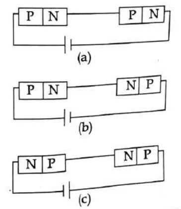
In the given circuits (a), (b) and (c), the potential drop across the two p-n junctions are equal in :
Every question from past board papers on p-n junction diode I-V characteristics, newest paper first. Open any question for its full worked answer.
In the given circuits (a), (b) and (c), the potential drop across the two p-n junctions are equal in :
The increase in the width of the depletion region in a p-n junction diode is due to :
In a p-n junction diode, change in temperature due to heating
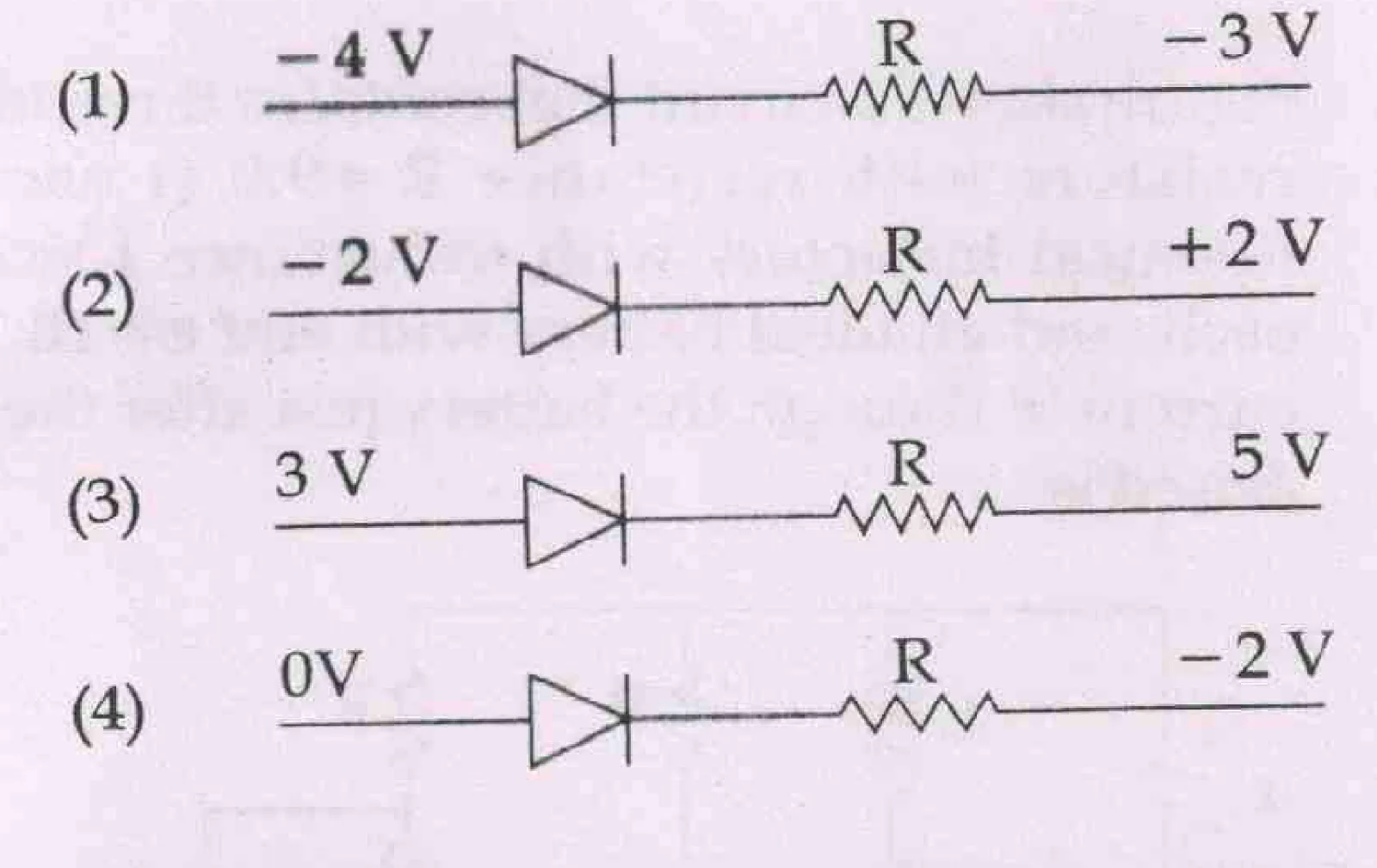
Which one of the following represents forward bias diode ?
Consider the junction diode as ideal. The value of current flowing through AB is :

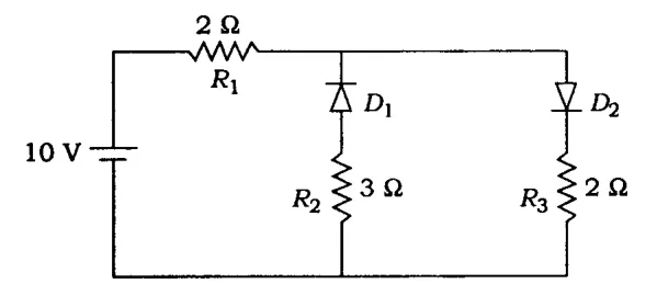
The given circuit has two ideal diodes connected as shown in the figure below. The current flowing through the resistance \(R_1\) will be